In the rapidly evolving landscape of electronic product manufacturing, PS injection molding has emerged as a crucial technology, enabling us to produce components that seamlessly blend functionality, durability, and aesthetic appeal. By leveraging the unique properties of polystyrene (PS) and the precision of injection molding processes, we can create parts that meet the stringent requirements of modern electronics, from safeguarding internal circuits to enhancing user experience. PS injection molding is playing an increasingly pivotal role in driving innovation and improving the overall quality of electronic products.
1. The Material Attributes of PS Injection Molding for Electronic Products
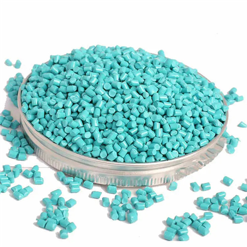
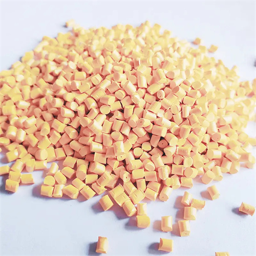
When we embark on the production of electronic products, the choice of PS for injection molding is based on its remarkable material characteristics. PS offers excellent electrical insulation properties, which are essential for preventing electrical interference and ensuring the proper operation of electronic devices. Its high dielectric strength allows PS – injection – molded parts to effectively isolate electrical components, reducing the risk of short – circuits and signal disruptions. This makes PS an ideal material for components that require reliable electrical isolation, such as insulators and casings for circuit boards.
Another significant advantage of PS is its high rigidity and dimensional stability. Electronic products often consist of numerous small and precisely – sized components, and PS – injection – molded parts can maintain their shape and dimensions with great accuracy. This stability ensures that parts fit together perfectly during assembly, preventing any gaps or misalignments that could affect the performance or durability of the product. Additionally, PS has a smooth surface finish, which is beneficial for both the aesthetic appearance of electronic products and for preventing the accumulation of dust and debris, which could potentially interfere with electrical components.
2. PS Injection Molding in Electronic Device Housings
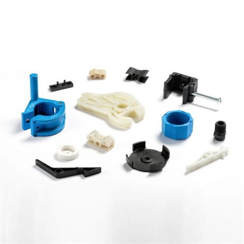
PS injection molding is widely utilized in the manufacturing of electronic device housings. The versatility of the injection molding process allows us to create housings with complex geometries and intricate designs. We can incorporate features such as ventilation holes for heat dissipation, ports for connectors, and ergonomic contours for better user grip directly into the PS – injection – molded housing, streamlining the assembly process and enhancing the functionality of the device.
For smartphones and tablets, PS – injection – molded housings offer a combination of protection and style. Their smooth surfaces can be easily customized with different textures, colors, and finishes, allowing us to meet the diverse design preferences of consumers. The rigidity of PS provides robust protection for the internal components, safeguarding them from accidental drops, impacts, and scratches. In larger electronic devices like laptops and desktop computers, PS – molded housings can also contribute to the overall structural integrity of the product while maintaining a lightweight profile, making the devices more portable and user – friendly.
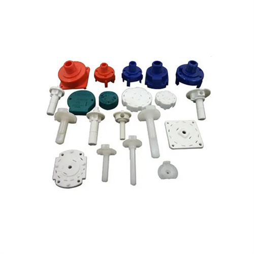
3. PS Injection Molding for Electronic Component Insulators and Connectors
In the realm of electronic components, PS injection molding plays a crucial role in the production of insulators and connectors. PS – injection – molded insulators are vital for preventing the flow of electrical current between different parts of a circuit, ensuring the safety and reliability of electronic devices. Their high electrical insulation properties make them suitable for isolating electrical wires, protecting sensitive components from electrical interference, and preventing short – circuits.
Connectors made through PS injection molding offer reliable electrical connections. The precision of the injection molding process allows us to create connectors with accurate pin placements and secure locking mechanisms. This ensures stable electrical conductivity and minimizes the risk of loose connections, which could lead to device malfunctions. Whether it’s the connectors for charging cables, data transfer interfaces, or internal connections within a circuit board, PS – injection – molded connectors provide a durable and efficient solution, contributing to the seamless operation of electronic products.
4. Precision and Cost – Efficiency of PS Injection Molding in Electronic Product Production
Precision is at the core of our PS injection molding processes for electronic products. Advanced injection molding machines, equipped with sophisticated computer – controlled systems, allow us to precisely regulate parameters such as injection pressure, temperature, and cooling time. When manufacturing small and highly intricate components, like the tiny insulators in micro – switches or the connectors for miniature circuit boards, we can fine – tune the injection process to achieve extremely tight tolerances. For example, the dimensions of PS – injection – molded connector pins can be produced with an accuracy of ±0.01mm, ensuring a perfect fit and reliable electrical performance.
Cost – efficiency is another significant benefit of PS injection molding in electronic product production. The relatively low cost of PS raw materials, combined with the high – volume production capabilities of injection molding, enables us to produce components at a competitive cost per unit. When manufacturing 100,000 PS – injection – molded smartphone back covers in a single batch, for instance, the economies of scale significantly reduce the production cost. The automated nature of the injection molding process also cuts down on labor costs, as computer – controlled machines handle most of the production tasks, minimizing the risk of human – error – related defects and ensuring consistent quality across all units.
5. Future Prospects of PS Injection Molding in the Electronics Industry
As we look to the future, we are excited about the potential of PS injection molding in the electronics industry. With the continuous advancement of technology, there is an increasing demand for smaller, faster, and more energy – efficient electronic devices. We anticipate the development of new PS – based materials with enhanced properties, such as improved heat resistance to better manage the heat generated by high – performance components, and enhanced mechanical strength to withstand more rigorous handling.
The integration of smart features into electronic products will also present new opportunities for PS injection molding. We expect to embed sensors, microcontrollers, and wireless communication modules into PS – injection – molded components, enabling features like real – time monitoring, self – diagnosis, and remote control. Additionally, as sustainability becomes an increasingly critical concern, efforts will be made to improve the recyclability of PS – molded electronic parts, reducing the environmental impact of electronic product production. These future developments will undoubtedly expand the applications and influence of PS injection molding, driving the continuous innovation and growth of the electronics industry.
